- 您现在的位置:买卖IC网 > Sheet目录3880 > PIC18F8621T-I/PT (Microchip Technology)IC PIC MCU FLASH 32KX16 80TQFP
2005 Microchip Technology Inc.
DS39612B-page 107
PIC18F6525/6621/8525/8621
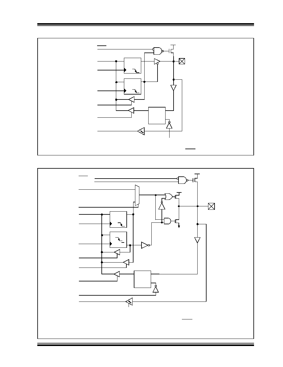
FIGURE 10-6:
BLOCK DIAGRAM OF RB2:RB0 PINS
FIGURE 10-7:
BLOCK DIAGRAM OF RB3 PIN
Data Latch
RBPU(2)
P
VDD
Q
D
CK
Q
D
CK
QD
EN
Data Bus
WR TRISB
RD TRISB
RD PORTB
Weak
Pull-up
RD Port
INTx
I/O pin(1)
TTL
Input
Buffer
Schmitt Trigger
Buffer
TRIS Latch
Note
1:
I/O pins have diode protection to VDD and VSS.
2:
To enable weak pull-ups, set the appropriate TRIS bit(s) and clear the RBPU bit (INTCON2<7>).
WR LATB or
WR PORTB
Data Latch
P
VDD
Q
D
CK
Q
D
EN
Data Bus
WR LATB or
WR TRISB
RD TRISB
RD PORTB
Weak
Pull-up
ECCP2 or INT3
TTL
Input
Buffer
Schmitt Trigger
Buffer
TRIS Latch
RD LATB
WR PORTB
RBPU(2)
CK
D
Enable(3)
ECCP Output
RD PORTB
ECCP Output(3)
1
0
P
N
VDD
VSS
I/O pin(1)
Q
CCP2MX
CCP2MX = 0
Note
1:
I/O pin has diode protection to VDD and VSS.
2:
To enable weak pull-ups, set the appropriate TRIS bit(s) and clear the RBPU bit (INTCON2<7>).
3:
For PIC18F8525/8621 parts, the ECCP2 input/output is multiplexed with RB3 if the CCP2MX bit is enabled (= 0)
in the Configuration register and the device is operating in Microprocessor, Microprocessor with Boot Block or
Extended Microcontroller mode.
发布紧急采购,3分钟左右您将得到回复。
相关PDF资料
XF2L-1835-1
CONN FPC 18POS 0.5MM SMT
XF2L-1535-1
CONN FPC 15POS 0.5MM SMT
PIC16LF767T-I/SO
IC PIC MCU FLASH 8KX14 28SOIC
XF2L-1335-1
CONN FPC 13POS 0.5MM SMT
XF2L-1325-1
CONN FPC 13POS 0.5MM SMT
PIC16F767T-I/ML
IC PIC MCU FLASH 8KX14 28QFN
XF2L-1235-1
CONN FPC 12POS 0.5MM SMT
PIC16LF74-I/ML
IC MCU FLASH 4KX14 A/D 44QFN
相关代理商/技术参数
PIC18F8622-E/PT
功能描述:8位微控制器 -MCU 8B Microcontrollers RoHS:否 制造商:Silicon Labs 核心:8051 处理器系列:C8051F39x 数据总线宽度:8 bit 最大时钟频率:50 MHz 程序存储器大小:16 KB 数据 RAM 大小:1 KB 片上 ADC:Yes 工作电源电压:1.8 V to 3.6 V 工作温度范围:- 40 C to + 105 C 封装 / 箱体:QFN-20 安装风格:SMD/SMT
PIC18F8622-I/PT
功能描述:8位微控制器 -MCU 64 KB 4K RAM 70 I/O RoHS:否 制造商:Silicon Labs 核心:8051 处理器系列:C8051F39x 数据总线宽度:8 bit 最大时钟频率:50 MHz 程序存储器大小:16 KB 数据 RAM 大小:1 KB 片上 ADC:Yes 工作电源电压:1.8 V to 3.6 V 工作温度范围:- 40 C to + 105 C 封装 / 箱体:QFN-20 安装风格:SMD/SMT
PIC18F8622-I/PTG
制造商:Microchip Technology Inc 功能描述:IC 8BIT MCU FLASH 18F8622 TQFP80
PIC18F8622T-I/PT
功能描述:8位微控制器 -MCU 64 KB 4K RAM 70 I/O RoHS:否 制造商:Silicon Labs 核心:8051 处理器系列:C8051F39x 数据总线宽度:8 bit 最大时钟频率:50 MHz 程序存储器大小:16 KB 数据 RAM 大小:1 KB 片上 ADC:Yes 工作电源电压:1.8 V to 3.6 V 工作温度范围:- 40 C to + 105 C 封装 / 箱体:QFN-20 安装风格:SMD/SMT
PIC18F8625-I/PT
功能描述:8位微控制器 -MCU 96kBF 4096RM 40MHz nonoWatt RoHS:否 制造商:Silicon Labs 核心:8051 处理器系列:C8051F39x 数据总线宽度:8 bit 最大时钟频率:50 MHz 程序存储器大小:16 KB 数据 RAM 大小:1 KB 片上 ADC:Yes 工作电源电压:1.8 V to 3.6 V 工作温度范围:- 40 C to + 105 C 封装 / 箱体:QFN-20 安装风格:SMD/SMT
PIC18F8625T-I/PT
功能描述:8位微控制器 -MCU 96kBF 4096RM 40MHz nonoWatt RoHS:否 制造商:Silicon Labs 核心:8051 处理器系列:C8051F39x 数据总线宽度:8 bit 最大时钟频率:50 MHz 程序存储器大小:16 KB 数据 RAM 大小:1 KB 片上 ADC:Yes 工作电源电压:1.8 V to 3.6 V 工作温度范围:- 40 C to + 105 C 封装 / 箱体:QFN-20 安装风格:SMD/SMT
PIC18F8627-E/PT
功能描述:8位微控制器 -MCU 96 KB FL 3936 RAM 25 MHz RoHS:否 制造商:Silicon Labs 核心:8051 处理器系列:C8051F39x 数据总线宽度:8 bit 最大时钟频率:50 MHz 程序存储器大小:16 KB 数据 RAM 大小:1 KB 片上 ADC:Yes 工作电源电压:1.8 V to 3.6 V 工作温度范围:- 40 C to + 105 C 封装 / 箱体:QFN-20 安装风格:SMD/SMT
PIC18F8627-I/PT
功能描述:8位微控制器 -MCU 96 KB 4K RAM 70 I/O RoHS:否 制造商:Silicon Labs 核心:8051 处理器系列:C8051F39x 数据总线宽度:8 bit 最大时钟频率:50 MHz 程序存储器大小:16 KB 数据 RAM 大小:1 KB 片上 ADC:Yes 工作电源电压:1.8 V to 3.6 V 工作温度范围:- 40 C to + 105 C 封装 / 箱体:QFN-20 安装风格:SMD/SMT